This is the followup article to my DIY stereo system where I will explain how I built the amplifier for my speakers that I have introduced in PART I.
Abstract
In this article, I will outline how I designed and built the amplifier for my speaker system. I will go over every aspect in a lot of detail and try to focus on the emerging thoughts behind my design decisions. This article is intended to teach and inform anyone who might also want to build their speaker system. The amplifier will be fully analog. There is only one exception: The power supply will not be built by me and not be analog, but a switching one. However, I intend to replace the power supply in the future with one that I build myself and I will probably write another article about that so stay tuned. This analog amplifier is not a classical one that amplifies all frequencies equally, but one that respects the frequency response of the speakers. Additionally, all filtering will be done before the power stage, which means that each speaker will be driven directly.
Overview
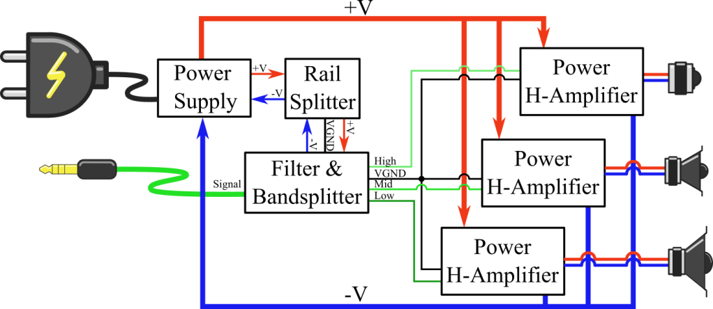
When designing a bigger and more complex system, like the amplifier, I like to sketch it out from the top first. That way the system can be split into independent modules that can then be built from the bottom up. In the following picture, the chosen amplifier topology can be seen. Note that H-Bridge amplifiers have been chosen for the power stage. H-Bridge amplifiers output two signals, the original and an inverted. Thus doubling the signal and quadrupling the power output adding a +6dB gain to the system. Additionally, the majority of the current will flow over the main power lines (+V, -V) and not into the ground line. This allows using a conventional power supply with only one output channel that provided lots of currents and an additional low power rail-splitter which creates a reference potential that can be used as a virtual ground (VGND).
In the following chapters, I will explain each module, how I designed them, what went wrong and how I got to the final product.
Filters
The filters in this amplifier fulfill three tasks. First, they amplify the signal. Second, they split the audio spectrum into three bands and try to minimize the phase margin between two speakers at the separation frequencies for a continuous take-over. Third, the filters will compensate for the frequency response of the speakers in the box.
We have already tried to reason about the frequency response in the previous article and how the amplifier might correct it. Now we are going to calculate the needed response of the amplifier. I want to point out, that we are not calculating the correct absolute values of the filters but merely their shape. Then we will design the filters to match the calculated response.
Shaping the Filters
The total system can be described as follows:
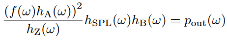
The input signal ‘f’ will be amplified by the filters ‘hA‘. At the speakers’ impedance ‘hZ‘ the signal will be transformed into power. If we then multiply this power output with the efficiency or sound-pressure-level ‘hSPL‘ and the behavior of the box ‘hB‘ we get the total power output density. Rewriting that formula in terms of dB simplifies the equation.

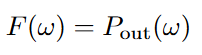
Now we demand that the output power ‘Pout‘ will follow the input signal ‘F’ in an un-distorted way:
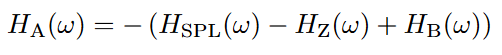
With this equation and resolving to ‘HA‘ we get the desired amplifier shape as follows.
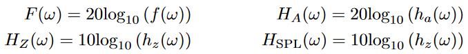
For the purpose of visualizing the equations we will further define the following expressions:

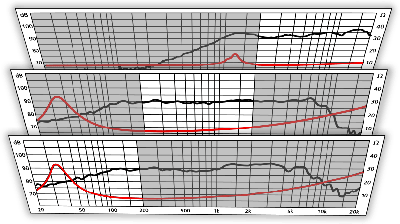
The graph below shows the calculation for the design frequencies of each speaker and it is very interesting to see how each part affects the system.
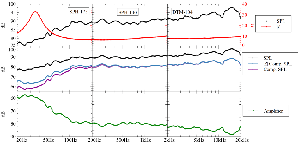
At the top of the graphs, you can see the impedance of the speakers ‘hZ‘ in red and their SPL ‘HSPL‘ in black. In the middle, you can see the impedance corrected output ‘HZCor.SPL‘ in blue. Notice how the impedance peak of the SPH-175 pushes the output down. Simulations of the speaker box showed that it behaves like a high pass with a -3dB frequency at about 70Hz. If we take the speaker box into account and correct the output accordingly we get ‘HCor.SPL‘ in violet. The desired shape of the amplifier ‘HA’ is then the inverse of the corrected speaker output and can be seen in green.
Designing the Filters
The filters are responsible to amplify the signal, splitting it into different bands for each speaker, and shaping the signal to correct for the speaker frequency response. To accomplish those tasks the filters have been split into three stages as shown below.
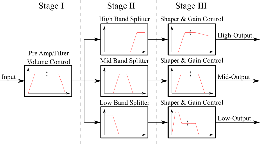
The diagram above shows that in the first stage the input can be variable amplified. Additionally, DC offsets will be blocked and very high-frequency noise suppressed. In the second stage, the signal will be split into the different frequency ranges that each speaker will play. The last stage will add a variable gain for each band and shape the signal to correct the behavior of the speaker and the box.
Stage I : Pre-Amp and Volume Control
Before we start to design the input stage we first have to know what our input is, which is not so trivial for audio. The most commonly used audio levels are:
- -10dBV for Consumer-Audio
- +4dBu for Pro-Audio
-10dBV describes the RMS voltage in dB. The RMS voltage ‘URMS‘, peak ‘Up‘, and peak-to-peak Amplitude ‘Upp‘ can be calculated as follows:

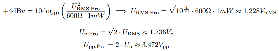
+4dBu is a bit more complicated and has a strong historic bias. 0dBu stands for a signal with a voltage that if it were connected to a 600Ω load would create a power output of 1mW. So the signal strength can be calculated to:
The input signal should be amplified as much as possible without clipping. This amplifier is a consumer product and mainly interacts with other consumer products so those levels are not allowed to clip. Furthermore, the pro levels should be supported as far as possible.
Now lets first make an input filter and then add an amplifier to it. The input filter should get rid of any DC-offsets that might be in the signal and additionally remove high-frequency noise.
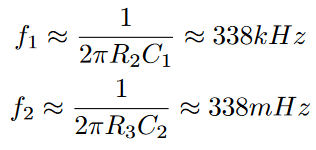
To the right, you can see a passive low impedance low-pass filter with R2 and C1 followed by a high impedance high-pass filter with C2 and R3. This cascaded passive filter works because the impedance of the high pass is so much greater that it won’t influence the low pass significantly which lets us easily create a 338mHz to 338kHz band-pass.
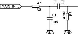
The frequencies of the input filters have been selected so far beyond the audible spectrum so that the phase of the input signal won’t be distorted too much.
To amplify the signal I chose the operational amplifier TL072. It is often referred to as a jellybean Op-Amp because it is very cheap, widely available, and often used within the industry. But don’t be misled by the name jellybean, because this OP-Amp performs. It has a lot of great features like its low noise of 15nV/sqrt(Hz), low harmonic distortions of 0.01%, and high slew-rates of up to 16V/µs which we need. Because, if we have a sine wave with a voltage swing of our power lines (in my case +-7.5V) at a frequency of 25kHz we already need a minimum slew-rate of:


We need a minimum slew-rate of 1.18 V/µs for just one sine. Having a 10 times faster Op-Amp is recommended.
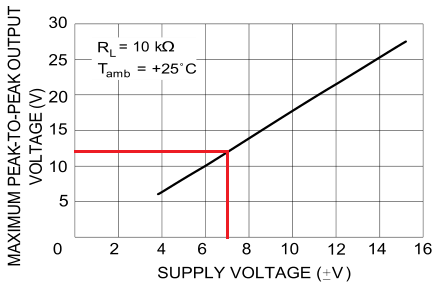
Now we need to figure out how much we can amplify the signal. In my case, I am using a 15V power supply. So when split into two I have a symmetric supply voltage of +-7.5V. A look into the datasheet of the TL072 shows us in Figure 7 that the maximum peak-to-peak output voltage for that supply is at about 12 to maybe 12.5V so that is what we are aiming for.
In the following schematic, you can see the added amplifier to the passive filter.
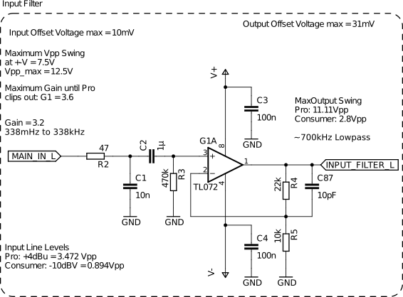
Firstly we want to amplify the signal so that the Pro level does not clip. The Voltage divider of R4 and R5 with 22k and 10kΩ results in a Gain of:
The Pro level of 3.472Vpp will then be amplified to about 11.11Vpp which is still below the maximum 12.5Vpp of the TL072
Additionally, C87 has been added to the feedback line so that high-frequency noise won’t be amplified.
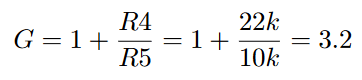
The Input filter is then directly followed by the volume control.
The volume can be controlled by the potentiometer P1A. It is a stereo-logarithmic one so changes feel natural to our ear. If P1A outputs 100% of the input signal, the amplifier will add a gain of 4.3. The pro level would hypothetically be amplified to 47.77Vpp but will clip at the voltage rails. The consumer level will reach a magnitude of 12.04Vpp which is within the tolerated bounds.
You may wonder why there is a dashed line around the potentiometer and why it is connected to ground. The potentiometers that I use are mostly made out of plastics but have a metal case or shielding around them that also provide thicker mounting pins for the PCB. In one of my earlier designs I did not connect them to anything and every time I turned them I could hear noise being coupled into the speakers. So in this design, I connect them to the Ground.
Stage II : Band-Splitter
For the band splitter, I used 4th order filters, because at their cutoff frequency, which is also the transition from one speaker to another, they have a phase of +-180°. When we then add a dampening factor that is smaller than 1 we can lift the amplitude so that we reach -3dB and +-180° at the cutoff frequency. This will result in smooth takeovers and the phase does not have to jump between the mounting points of the speakers.
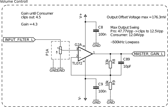
We will try to reduce the number of Op-Amps to a minimum and only use one per 4th order filter. This can be achieved by using two passive 1st order filter stages followed by an active 2nd order one where each stage has an impedance increase by about a magnitude of 10.
High Band
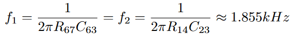
The following schematic shows the high pass filter for a design frequency of 2kHz with two passive 1st order filter followed by a 2nd order Sallen-Key filter.
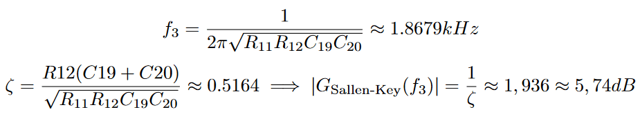
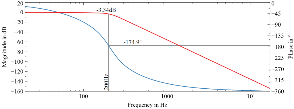
The cut of frequencies of the individual filters has been set slightly below the design frequency. This has been done so that the amplitude of the design frequency is not too low and together with a dampening factor of 0.06 the (-3dB, -180°) point was approximated at 2kHz, as can be seen in the following bode diagram.

Furthermore, I want to analyze the individual filters. The cutoff frequencies ‘f1‘ and ‘f2‘ of the passive filters can be calculated to:
The cutoff frequency ‘f3‘ of the Sallen-Key filter as well as its dampening ‘ζ’ can be calculated to:
Low Band
The 4th order low-pass filter can be designed very similarly by just switching the capacitors and resistors as seen below.
The passive filters have a cutoff frequency of:
The Sallen-Key parameters can be calculated to:
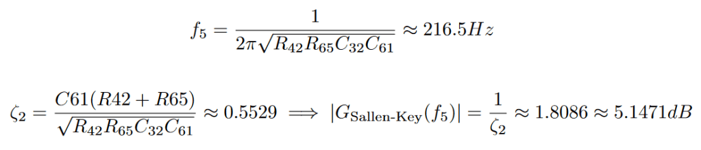
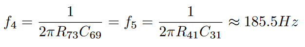
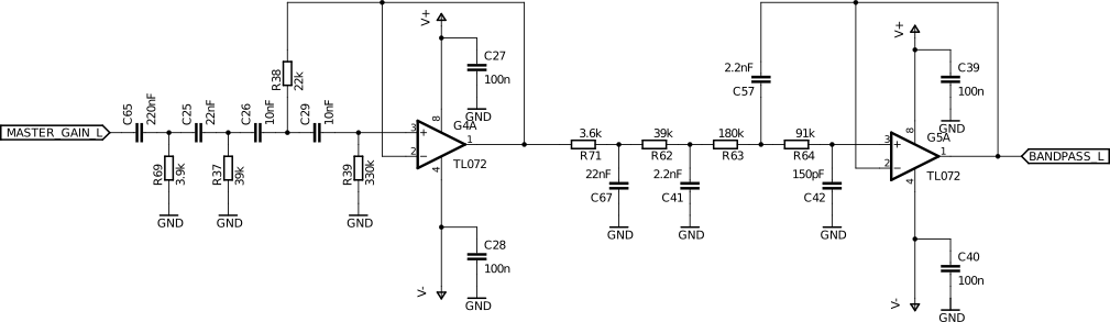
Mid Band
In order to separate the mid band, we are going to use a 4th order band-pass that will be using the previous designs. The filters above are amazingly versatile. We can just multiply a factor to all capacitors and the frequency will change by the same amount. The dampening of the filter, however, will be left unchanged. The schematic and its bode diagram of the band-pass can be seen below:
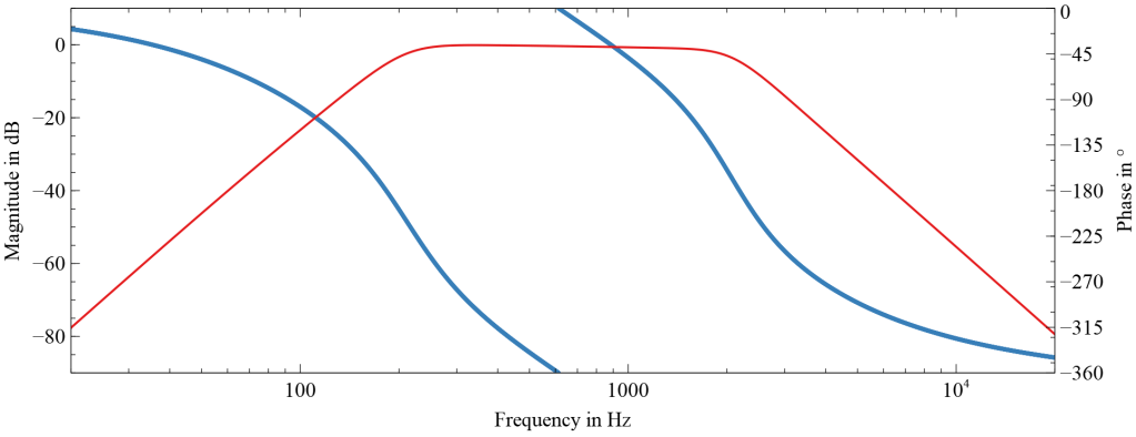
The phase progression in the above bode diagram is of course continuous. It just seems to jump because the phase in the picture above has been plotted modulo -360°.
Stage III : Shaper
The shapers are responsible to correct the frequency response of the system and create a flat system response. A calculated frequency curve for each speaker band has already been shown in figure (3). In the following schematics, we will approximate those with iterative filter designs. Furthermore, potentiometers have been added to control the gain of each band. Additionally, At the output stage, the signal will be amplified one last time before it goes into the power amplifiers.
But by how much can we amplify the signal of each band without clipping? This is a non-trivial question, because the input signal is indirectly (with the unit VRMS that represents the DC voltage for any signal that dissipates the same power over a load with no imaginary parts) related to a power frequency distribution. So if we filter frequencies away we can consider that the peak-to-peak voltage is going to drop. In this article, we are going to assume that the energy flow density is logarithmically distributed. So we can guess that each of our bands (which are logarithmically spaced) carries 1/3rd of the signal strength.
Additionally, we want the output to be optimized for when the band-gain-potentiometers are in their middle position. This is done to grant the possibility to easily amplify or reduce the gain of each band. At no time should the user of the amplifier feel the need to turn up all frequency bands in order to add more volume.
In the middle position, my specific potentiometers have a resistance ratio of about 10kΩ : 40kΩ. This means that the potentiometer divides the input voltage by 5.
So overall the signal will be reduced by a factor of 3 * 5 = 15 which means we are going to amplify it by the same amount.
So after all that lets finally start designing the shapers.
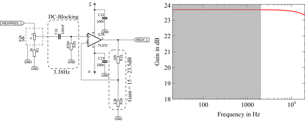
High Band Shaper
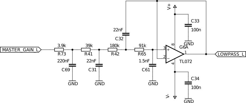
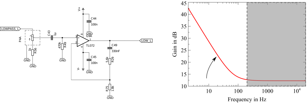
First, we want to add a Gain of 15 as seen in the following schematic. Since this is the output stage of the filter system and we amplify the signal by a large amount it is a good place to also add some DC-Blocking that might have been accumulated by previous Op-Amps. Therefore, a capacitor C11=100nF has been chosen because it is already widely used in the whole schematic, and a resistor R20=470k impedes any buildup of static charge. The resistor is also large enough to not affect the potentiometer P2A.
The DTM-104 High band tweeter is a little bit louder in the higher frequencies as previously shown in figure 3. Thus we will dampen them by reducing the impedance between the Op-Amp output and the feedback line. We can do so by adding a capacitor C73 and a resistor R77 as shown in the next schematic.
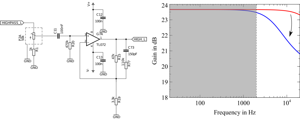
In the above diagram with an ideal Op-Amp and very low frequencies, the capacitor C73 has a very high impedance. One can think of it as an open. At very high frequencies C73 has a very small impedance and R15 and R77 are basically in parallel with a total resistance of ‘Rp‘:

This will give us this nice and long amplitude roll-off with a 3dB dampening around the frequency:
Since this is the high band speaker we want to make sure not to amplify any unnecessary low frequencies. We can prevent the Op-Amp from amplifying low frequencies with a gain of 15 by increasing the impedance between the feedback and ground with another capacitor C79.

This will suppress low frequencies and DC components to a minimum of 0dB.
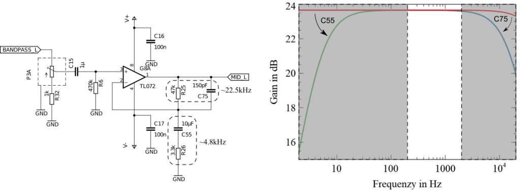
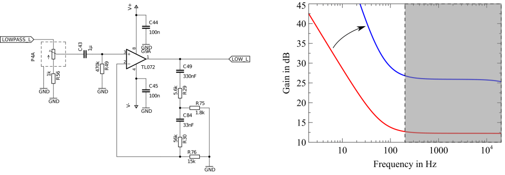
Mid Band Shaper
The mid Band does not need a lot of adjustments and the frequency curve can be left at a constant Gain. Nevertheless, this is another good opportunity to reduce potential noise instead of amplifying it. So two capacitors have been added to create a band-pass filter.
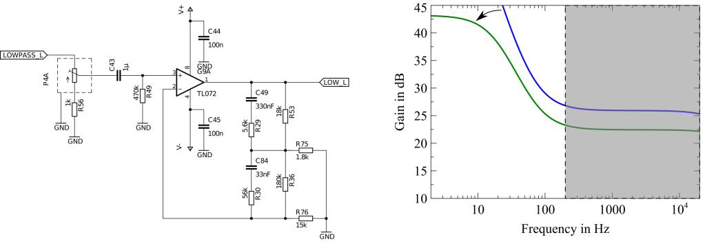
Low Band Shaper
As seen in figure 3 the very lows need to get amplified. This can be achieved by an low pass filter. An active feedback low-pass can be realized with a high pass in its feedback loop as seen in the following picture.
A single high-pass filter in the feedback loop will only create a 20dB increase in magnitude per decade. However, if you carefully study figure 3 you notice that a 40dB increase is needed. Using the same high-pass filter twice in a row will give us exactly that as can be seen below.
There is only one small problem, DC offsets will now be theoretically amplified by infinity. To limit this resistors can be placed in parallel to the capacitors, which will generate the output that can be seen in figure 18-c.
Just limiting the DC gain is nice but it would be better to reduce the DC gain as far as possible. To reduce the DC gain even further Capacitors C85 and C86 can be added to the schematic which will then give the frequency response as shown in figure 18-d.
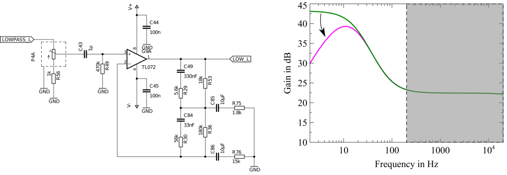
As a final touch, a capacitor C77 can be added that connects right in between the output and the negative feedback of the Op-Amp. This will reduce the gain for high frequencies.

Filter Layout
In the following picture (figure 19) you can see the layout of the filters that have been discussed above. I do not want to go into too much detail here but highlight one specific part.
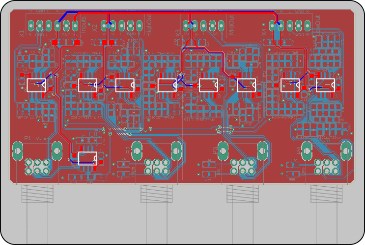
red – top layer
blue – bottom layer
This amplifier uses a switching power supply that generates quite a lot of high-frequency noise, that should, if possible, not be coupled into the signal lines. In electronics, there is often a misconception, because currents do not follow the path of least resistance, as often said, but of least impedance. This means that high-frequency currents will follow the paths with minimal field distance and the Energy is not carried by the wires but in the dielectric between them. If you want to learn more about noise and how to control it in your PCB design there is a great presentation by Rick Hartley at the Altium Keynote from 2019: Keys to Control Noise, Interference and EMI in PC Boards. To make sure that signals do not couple into each other I placed a large ground layer on the bottom and tried to make all routing on the top layer. This ensures that the electric fields have very short paths and are mostly in the dielectric of the PCB and do not radiate as much. Furthermore, you can see the highlighted power traces that are routed very closely together so that they too have short paths in between them, and the fields do not stray as much. The long signal traces have also been placed as far away from the power lines as possible. Additionally, I have made sure that there is always at least a ground trace between power and parallel signal traces on the same layer. There are also no large loops in the power traces.
H-Bridge Power Amplifier
So far all signals were created by devices that support currents of <50mA. If we want to drive the speakers that have an impedance of about 8Ω at a peak voltage of ~12V an output current of 1,5A is needed. So we need to massive increase our current output.
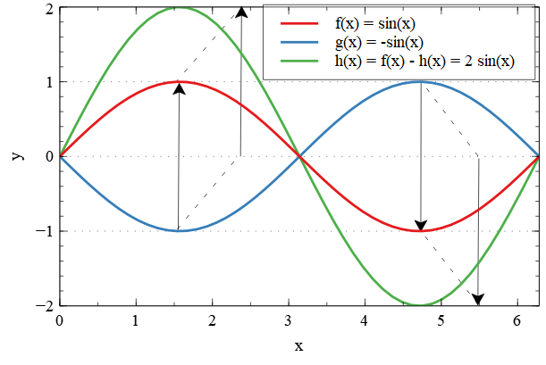
In this chapter, I want to explain how to design an H-Bridge or balanced power amplifier. The advantage of a balanced output compared to a single output is that both outputs can push and pull currents from both power lines – effectively doubling the amplitude of the signal. The following picture shows the effect of a sine wave (red) that has been added with its inverse (blue) which results in a sine that doubled in amplitude.
First I would like to discuss an amplifier type that is commonly used and did not work for my purposes and second I would like to show the thought process behind the working version that I ended up with.
Version 1
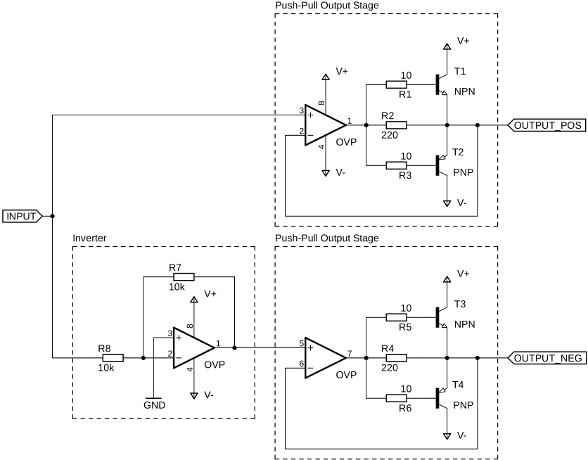
The first version of my power amplifier started from a classical AB-Push-Pull output stage with active feedback as can be seen in the following picture.
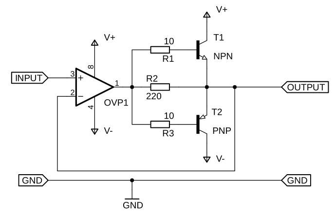
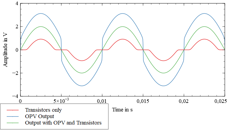
The transistors T1 and T2 in the above output stage are both used as emitter followers. They have the amazing ability to multiply the input current which flows through R1 and R3 into their base. The current multiplication factor is called B, β, but also often named hfe in Datasheets. While amplifying the current the transistors are maintaining the same voltage at their emitter as is presented to their base, minus the np-junction drop voltage (UBE). To overcome the np-junction voltage an OPV has been added which corrects this non-linear behavior. As an example, you can see a 100Hz 1V sine wave at an 8Ω load inputted into just the transistors without the OPV in red. It is clear to see how the sine wave disappears into the time-axis. Now adding the OPV you can see its output in blue and observes how it tries to compensate for the transistors to generate the desired output in green.
What I thought at that time was, that I can just invert the signal and feed it to a second output stage to create a balanced output. This is displayed in the following schematic:
The positive and negative output could then be connected to a load or speaker. This seemed to be a good idea. However, above a certain amplitude when connected to the speaker the amplifier would start to randomly make strange noises that sound similar to a scratched vinyl record. When measuring the output of the amplifier with an oscilloscope (see the picture below) something interesting can be observed.
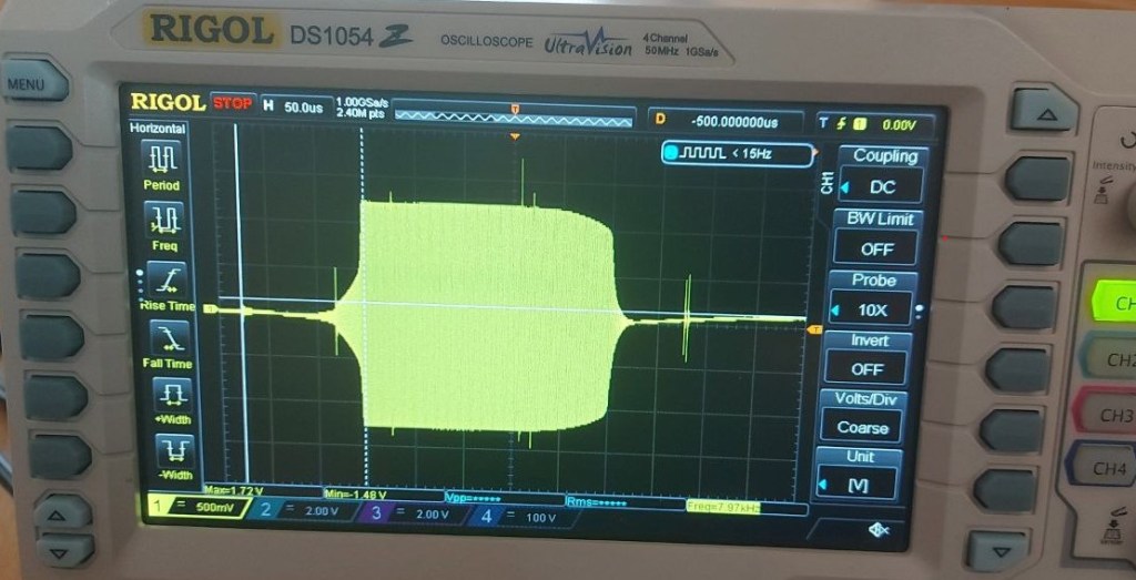
The amplifier oscillates for a relatively long time until it reproduced the signal again. The small spikes at the very beginning and after the big oscillation can be ignored for now, they are just noise from the switching power supply. I tried this with two different Op-Amps, the TL072 which I have also used for the filters, and the NE5532 which supports higher output currents and both created those distortions. It is also interesting to note that the oscillations would only start once the speakers were connected and sometimes the OPVs would have a DC offset and a measurably high voltage difference at their positive and negative input pins. Lesson learned, creating a balanced output using two parallel feedback systems can lead to instability issues. So I needed a fundamentally new design to realize the power amplifier. This leads us directly to version 2.
Version 2
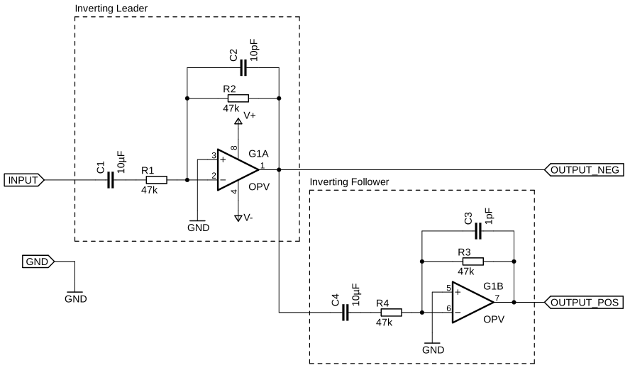
In the first version, I tried to use two parallel amplifiers, which did not work out. So in this new version, I cascade them. Because the final result may be quite difficult to understand at once, I am going to build it step by step. The main idea behind this is that one amplifier is following while the other one is leading the power output. This time, instead of implementing non-inverting I used inverting ones as can be seen in the following schematic.

In the above picture, both amplifiers will react equally fast to changes in their input. In order to successfully cascade them the follower needs to be significantly faster than the leader. Additionally, the leader needs to be significantly faster than the audible spectrum to reproduce it correctly. Adding a 10pF capacitor to the feedback line of the leader will slow it down to a frequency of 338kHz. The feedback line of the follower could be left unchanged, but adding a 1pF capacitor will reduce high-frequency noise by limiting its bandwidth to 3.38MHz which is still 10 times faster than the leader. Furthermore, DC-blocking capacitors have been added to the input lines all of which can be seen in the schematic down below.
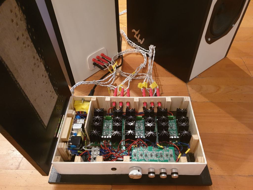
If we now add a push-pull output stage to each Op-Amp, heat-sinks to reduce the temperature of the transistors, decoupling capacitors, and fly-back diodes, the amplifier is finished.

In the picture above you can see the added components. I tried the new version again with the TL072 and the NE5532 and the issue with the oscillations and the offset that I had in my version 1 seemed to be gone. However, after a certain input voltage amplitude, the TL072 would again start to oscillate while the NE5532 remains stable. So I went with the NE5532. I tried to figure out why the TL072 would act as it does but even after studying the datasheets, I would not know why. To gain further knowledge I started simulations with SPICE models of the TL072 and they did not manage to reproduce my measurements.
Power Rail Splitter
All the filters and amplifiers that have been discussed so far use the ground as a reference around which the signals will be amplified. Most power supplies and also the ones that I use only have a negative and positive output. This means I either need a second power supply that I connect in series to create three different equally spaced potentials or I have to create it myself as described below.

The power rail splitter, as seen in figure 27-a, is just a push-pull output stage that tries to keep the output (the virtual ground) exactly in the middle of the two input lines. Resistors R9, R10, R11, and R12 have been placed to help the transistors dissipate power. Two transistor pairs are used, one would be enough but the calculated dissipated power comes very close to Ptot in the datasheet. So just to make sure that the SMD Transistors are not going to blow up during normal operations two transistor pairs have been placed in parallel.
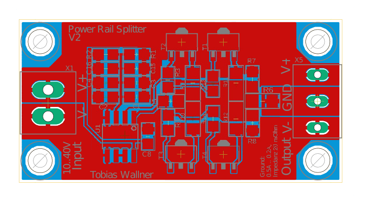
In an ideal scenario, all voltage levels are completely DC in the power rail splitter. However, you have to deal with some current. Wide traces and polygons provide sufficient copper in that regard as shown above in figure 27-b.
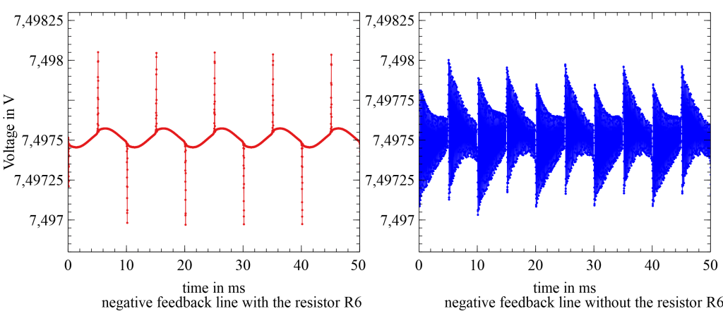
Since the output is very capacitive the resistor R6 has been added after the Feedback line to stabilize the OpAmp. Otherwise, it may start to oscillate at high frequencies which may drive the push-pull transistors noticeably hot. One would think that the small resistor R6 of 20mΩ does not do much, but the following comparison shows how important it is. The following voltages have been acquired between the negative supply and the negative feedback of the OpAmp with and without the resistor R6 while the speakers play a loud 100Hz tone at full swing.
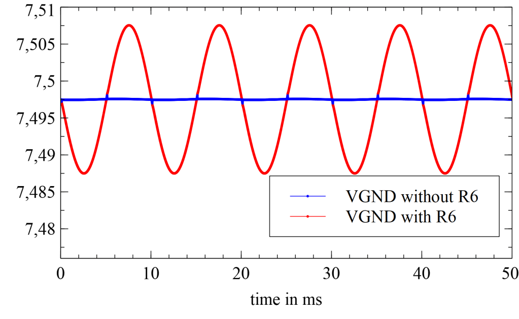
But as always nothing comes without a drawback. While the added resistor R6 can decrease high-frequency noise that would have been introduced into the, we lose a lot of ground precision as seen in the following overlay between the virtual ground outputs with and without the output resistor.
The final product
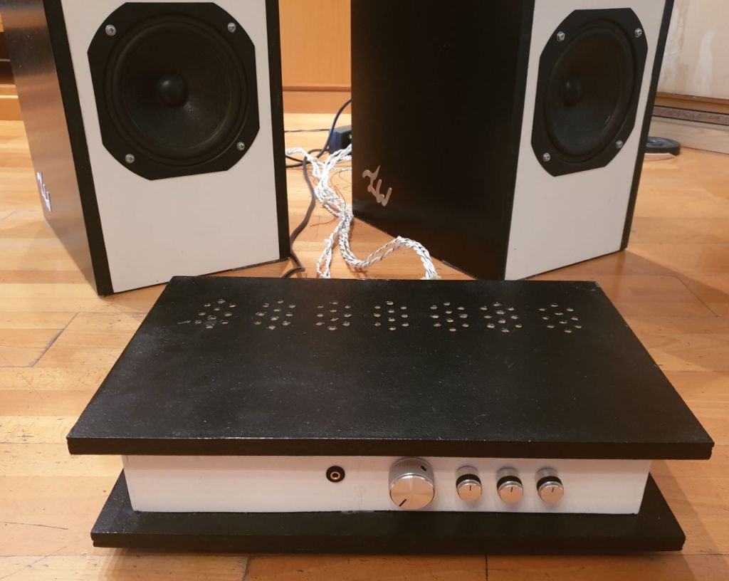
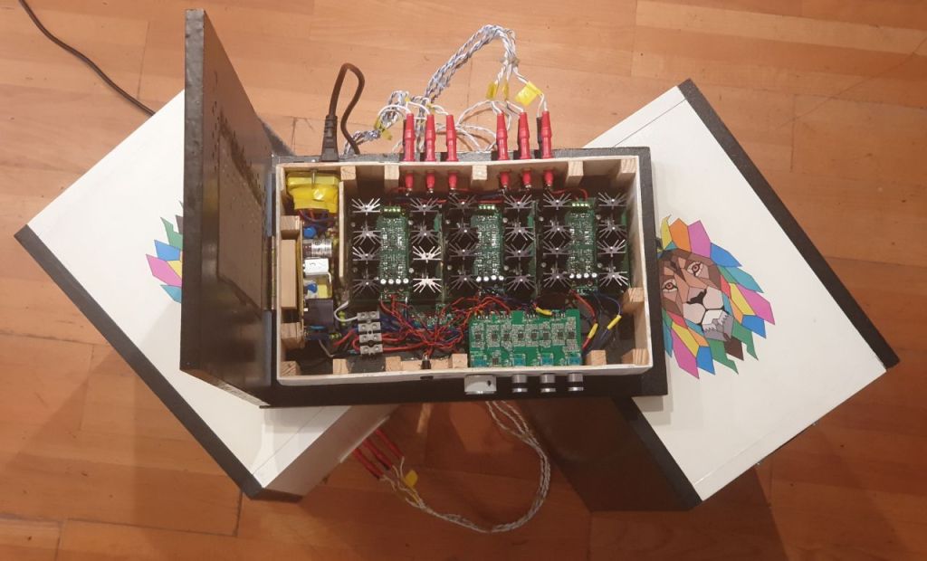
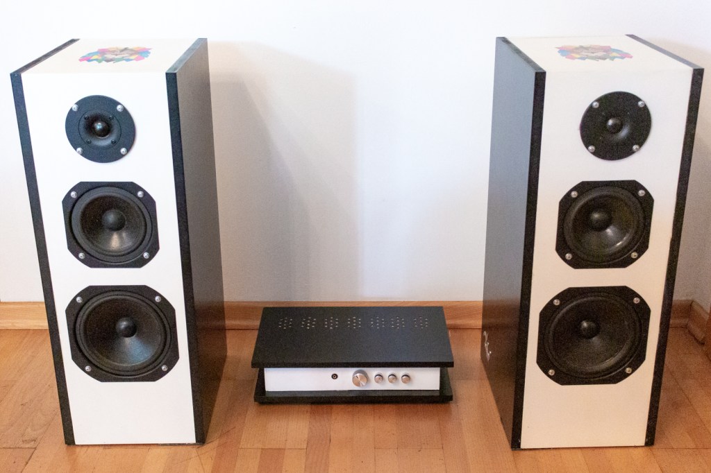

A lot of thought has been put into this speaker system and in retrospect, it was truly a unique experience and fun to build. But it was not all as easy and straightforward as it may have seemed. There were moments when I was on the brick, just about to quit it, because I could not figure out why something would not work as expected. Luckily I did not give up and pushed through until I had the speakers of my dream.
In the end, I want to thank my parents who let me use their living room as a laboratory for my experiments and the TU Wien university for letting me borrow their thermal camera to spot an error on one of the printed circuit boards.
For my next project, I would like to design a purely digital version of this analog amplifier. But for now, I will focus my time on my master’s in embedded systems engineering which is about to start in the 2022 winter semester.

Leave a comment